


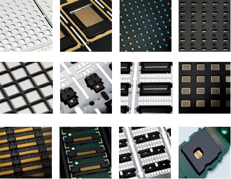
OpenMolding encapsulation process needs to expose the chip sensing area at the same time to protect the fragile bonding line plastic sealing, compared with the traditional packaging technology, at the beginning of the chip design OM needs to give full consideration to the chip pads and the location of the schematic sensing area to ensure that to meet the requirements of the OpenMolding process at the same time as possible to improve wafer utilisation; package design, the need to be specifically designed for the chip to match the plastic sealing tooling. In terms of encapsulation design, it is necessary to design a matching sealing mould for the chip; in terms of encapsulation process, in addition to the more demanding DieBond positional accuracy, at the same time, it is necessary to match the corresponding MoldReleaseFilm and sealing process parameters to ensure that there is no damage to the chip at the same time, there can be no air bubbles/plastic sealing folder breakage abnormalities, and moreover, there can be no chip sensing area overflow abnormalities.
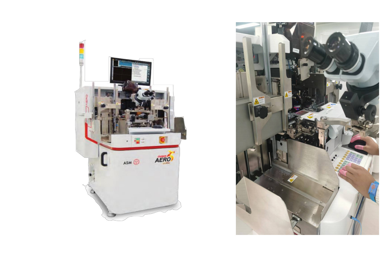
Automatic lead stitching machine
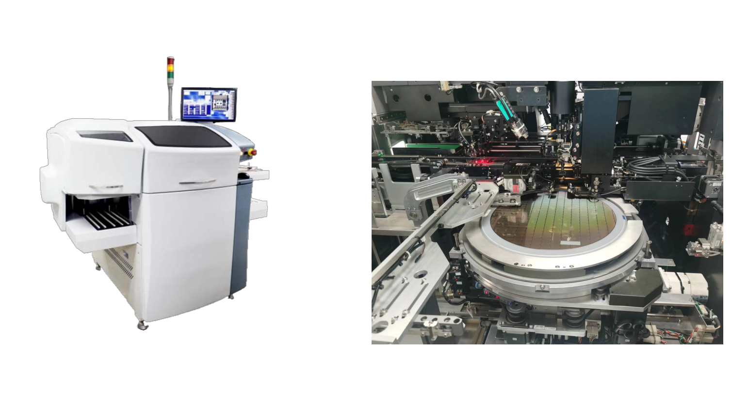
Fully automated fixed wafer machines